Breakthroughs in nanotechnology: lenses, robots, memory, and photonics
Korean metalenses, German nanorobots, Chinese DDR5, and American on-chip fiber optics
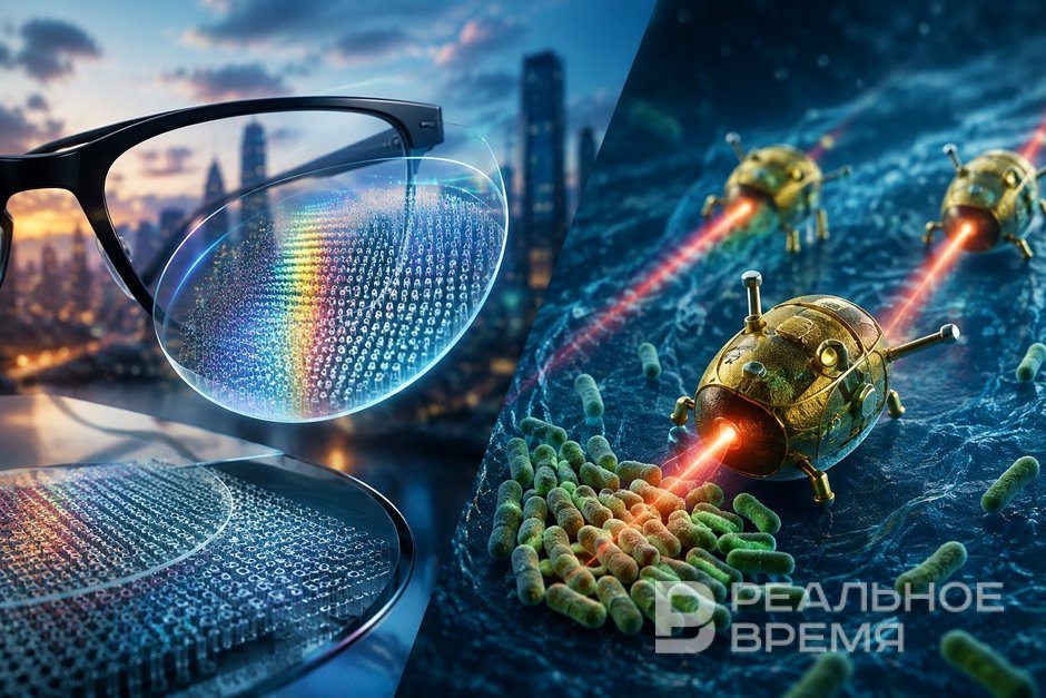
Over the past few months, several research groups have presented breakthrough developments: from flat lenses for augmented reality glasses to nanorobots that collect bacteria, from Chinese DDR5 memory catching up with global giants to fiber optics transferred onto a silicon chip for the first time. In Realnoe Vremya's technology digest — on how nanotechnology is getting closer to everyday life.
Nanolenses for future glasses: scientists found a way to eliminate color halos and launch mass production
Two independent studies by Korean engineers, published in Nature Communications, bring the era of lightweight augmented reality glasses closer. They managed to defeat the main enemy of flat lenses — rainbow fringes — and at the same time find a way to stamp such lenses by the thousands, like plastic cards. Imagine that instead of the usual thick glass in VR glasses, a transparent film no thicker than food wrap is used. This is precisely the goal that developers of metalenses are pursuing — flat optical elements covered with microscopic pillars called meta-atoms. These pillars work like tiny antennas, bending light as the engineer intends.
However, this technology had a serious “childhood disease” — chromatic aberration. In simple terms, blue, green, and red rays passing through such a flat lens focused at different points. As a result, the image separated into individual color outlines, like a misprint in a printing house. Professor Junsuk Rho's team from Pohang University of Science and Technology (POSTECH) found an elegant way to cheat this optical problem. Instead of using complex, expensive materials, they decided to play with the “height” of the nanostructures. Previously, engineers could only change the width of the pillar. Now, having mastered two-photon 3D printing technology (a kind of microscopic printer), they gained the ability to control height as well. It's like having Lego bricks not only of different widths but also of different floor heights. Thanks to this, each cell of the lens became “smart” — it is individually tuned so that all three colors meet strictly at one point. In laboratory conditions, such a lens, combined with an OLED screen, produced a clear full-color image without color halos.
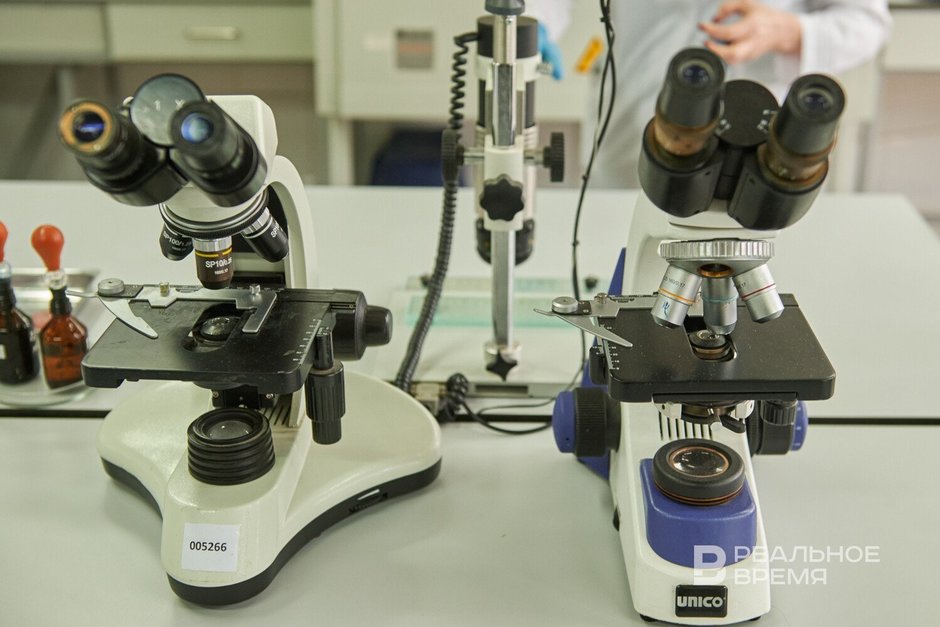
But printing one perfect lens on a 3D printer is one thing. How do you make a million such lenses for the mass market? The second study by the same team is devoted to solving this very problem. They created a special “template” (master mold) using electron-beam lithography. This technology allows drilling holes of varying depths in silicon. This rigid template is then used as a mold for casting transparent resin. The trick is that the imprint from such a template transfers not only the pattern but also the complex relief with varying heights. It's like being able to make a copy not of a flat photograph but of a bas-relief where all figures have different heights. The technology, called nanoimprint lithography, allows literally “stamping” lenses, which is critical for reducing production costs.
Professor Rho explains: “These studies are significant because they demonstrate manufacturing technologies capable of bringing full-color achromatic lenses for AR and VR displays to industrial use.” The prototypes created so far show focusing efficiency of about 27–33% — an excellent result for a start, although still far from the theoretical limit. Scientists still need to solve the problem of delivering such fragile nanostructures into real devices. Nevertheless, this discovery gives engineers a powerful tool: they now know that height can and should be used as a lever for controlling light. This means that in the near future, augmented reality glasses could indeed become lighter than a smartphone, and their image will no longer blur into separate colors, making the digital world truly real.
DOI: https://doi.org/10.1038/s41467-026-73103-2
DOI: https://doi.org/10.1038/s41467-026-73940-1
Laser “scoop” for the microworld: nanorobots learn to gather bacteria into dense swarms and transport them on command
German physicists have created tiny machines about 920 nanometers in size — roughly 50 times thinner than a human hair — that can catch, gather, and transport living bacteria, controlling them with just a laser beam. Scientists from the University of Würzburg, led by Professor Bert Hecht, published their results in Nature Communications. The main engineering challenge in creating such microscopic devices is how to make them move in a viscous liquid where Brownian motion constantly knocks them off course. The researchers found an elegant solution, using the recoil force from individual photons of light. Gold nanoantennas are placed on the robot's surface; they intercept photons and redirect them in one direction. Since the robot's mass is negligibly small (only 0.26 picograms), even such microscopic “recoil” accelerates it to 50 micrometers per second — in the nanoworld, this is comparable to sprinting.
However, speed without control is chaos. To make the robot go where needed, engineers added a self-aligning system to its design. The gold nanorods inside the robot act like a compass needle: they tend to align along the polarization direction of the incident light. By changing the laser polarization from horizontal to vertical, scientists make the robot turn 90 degrees, like a helmsman turning the wheel. For sharp maneuvers, a short pulse of light with circular polarization is used — it gives the robot an additional rotational impulse, allowing it to make clear turns without errors. As a result, the robot can trace complex trajectories, literally drawing letters and spirals with light, methodically scanning space like a nanovacuum cleaner.
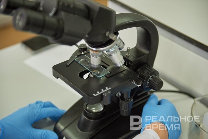
The most amazing part begins when such a robot is launched into a drop of water with bacteria. The plasmonic antennas not only push the robot forward but also slightly heat the surrounding liquid — by less than 10 degrees Celsius, which is safe for living cells. This local heating creates a thermophoretic force that acts like an invisible funnel, pulling bacteria toward the robot's surface. The bacteria do not stick chemically but are held by the external field, so the process is fully reversible. The robot can gather a dense swarm of dozens of microorganisms around itself, hundreds of times heavier than the device itself, and then, by switching polarization, transport this entire “living cargo” to another point and release it by simply turning off the laser.
In experiments, the robots successfully captured two types of bacteria — rod-shaped E. coli and spherical Staphylococcus — and both types arranged themselves into neat dense structures resembling ball packing. The robots remained fully controllable even with such a load, although their speed decreased due to increased water resistance. The authors emphasize that this is not just a toy. Traditional optical tweezers used for manipulating bacteria require hundreds of times higher laser intensity and can damage cells. The new method works at gentle power levels and allows processing not one, but many bacteria simultaneously.
Essentially, this is the first step toward creating microscopic “orderlies” capable of selectively cleaning biological samples from unwanted microorganisms or, conversely, delivering useful bacteria to the right place — for example, for targeted delivery of probiotics or in creating complex biofilms. The developers are already thinking about how to control an entire fleet of such robots using special spatial light modulators that split one laser beam into many independent “leashes.”
DOI: 10.1038/s41467-026-70685-9
Chinese DDR5 memory breaks the 9000 MT/s barrier for the first time — and this could change the component market
Chinese chip manufacturer CXMT (ChangXin Memory Technologies), together with partner Colorful, set a new record for memory on domestic chips: a 48 GB kit (2×24 GB) was overclocked to 9014 MT/s on a Colorful iGame X870E VULCAN W OC motherboard with an AMD Ryzen 9 9950X3D processor. This event is noteworthy not just for the numbers — it comes amid an acute DRAM shortage, when global leaders Samsung, SK Hynix, and Micron are shifting their capacities to produce expensive memory for AI accelerators, leaving ordinary users and PC builders with rising prices for DDR5 modules. In just a few months, Colorful engineers successively reached 8600, 8800, and now 9000 MT/s, with each time the system passing the rigorous RunMemTestPro stress test for stability, suggesting not a lucky batch but technology maturity.
However, speed is only part of the story. CXMT memory is beginning to match the top solutions of the “big three” in another key parameter — latency. In tests on ASUS boards, DDR5-6000 kits ran with CL30 timings, and in preliminary experiments, engineers even achieved CL28. For comparison, most retail CXMT modules today offer CL36 at 6000 MT/s, but the very fact that Chinese chips are capable of tight timings means the performance gap is rapidly closing. It's as if a budget car suddenly showed sports car dynamics — so far only on the track, but the potential is obvious.
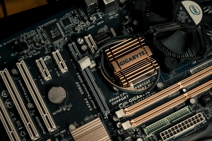
Beyond laboratory records, there are also real steps toward the mass market. Gigabyte has officially announced full compatibility of its DDR5 motherboards with memory on CXMT chips. Modules under the brands Asgard, Gloway, and KingBank are already being sold at retail at speeds of 5600–6000 MT/s. HP, ASUS, and Acer have begun installing such memory in some laptop models. In the first quarter of 2026, CXMT ranked fourth among global DRAM suppliers with a 7.6% share, and the price gap with the leaders has narrowed to 5–10%, making Chinese memory increasingly attractive to mass consumers.
Of course, a full “rescue” of the market is still far off. The record overclock to 9000 MT/s is manual tuning on a specialized board, not a mass specification, and CXMT's mass modules still run at modest 6000 MT/s with not the tightest timings. Moreover, CXMT's share in global supplies, though growing, still lags behind the industry giants. However, amid the DRAM shortage caused by the shift of capacities to the AI sector, it is precisely such successes that give the market hope for a real alternative in the coming years. If the Chinese manufacturer can transfer its record achievements to mass-produced products, gamers and enthusiasts will finally have a choice, and DDR5 prices will cease to depend solely on the will of the three largest vendors.
Fiber optics on a chip: new material reduces light loss by 20 times and brings quantum technologies closer
Engineers at the California Institute of Technology have learned to transfer the unique properties of optical fiber — record-low light loss — to silicon microchips. In a paper published in Nature, Professor Kerry Vahala's team describes a platform for photonic integrated circuits based on germanosilicate glass, which conducts light from violet to infrared with losses comparable to fiber optics. This achievement allows creating complex optical circuits on standard silicon wafers that previously required bulky glass components, and opens the door to ultra-precise optical clocks, quantum computers, navigation gyroscopes, and energy-efficient communication in data centers.
Optical fiber transmits signals over thousands of kilometers thanks to exceptionally pure glass and perfectly smooth internal surfaces — light is almost never scattered or absorbed. However, when engineers tried to do the same on silicon chips, they encountered insurmountable obstacles: traditional materials for photonic integrated circuits, such as silicon nitride, lost a lot of light, especially in the visible range where atomic clocks and quantum processors operate. The Caltech scientists solved this problem by using the same material as optical fiber — germanosilicate glass — but in the form of planar waveguides printed directly onto a silicon substrate using standard CMOS-compatible processes. The thickness of such waveguides is only 4 micrometers, and their sidewalls, after special annealing, become almost atomically smooth — like industrial optical fiber.
Measurements showed stunning results. Ring resonators on the new platform achieved quality factors exceeding 180 million across the entire range from 458 nm to 1550 nm, and at 1064 nm, this figure rose to 463 million, corresponding to losses of just 0.08 dB per meter — almost like the first commercial optical fiber created by Corning in 1970. In the violet region (458 nm), losses were 0.49 dB/m, which is 13 dB (20 times) lower than the best world analogues on silicon nitride. Moreover, some devices maintained ultra-high quality even without thermal treatment, which is extremely important for co-integration with temperature-sensitive components such as III-V lasers or thin-film lithium niobate.
The new platform demonstrated its versatility in three key applications. First, scientists created soliton microcombs — optical frequency combs with hundreds of equally spaced frequencies — in a single ring resonator with anomalous dispersion, which was previously impossible on ultra-high-Q nitride platforms without complex composite structures. Second, germanium doping allowed simultaneous confinement of acoustic waves in the waveguide core, leading to stimulated Brillouin laser generation with high coherence — opening the path to compact gyroscopes and ultra-sensitive sensors. Third, the large mode area in thick waveguides significantly suppressed thermorefractive noise, enabling injection locking of commercial laser diodes to microring resonators to achieve record narrow fundamental linewidths: 15 Hz at 632 nm, 12 Hz at 512 nm, and even 90 Hz at 444 nm — more than 20 dB better than current integrated visible lasers.
According to co-author Hao-Jing Chen, “this result surpasses the best world figures on silicon nitride by about 20 times, and there is still potential for further improvement.” Indeed, the theoretical loss limit for germanosilicate is about 0.2 dB per kilometer, corresponding to a quality factor of over 100 billion, and the authors are confident that further optimization of deposition and etching processes will approach these values. This means photonic integrated circuits could soon compete with fiber optics not only in quality but also in cost, as they will be manufactured on standard CMOS fabs.
A tenfold reduction in losses provides a hundredfold increase in laser coherence, which is critical for optical clocks, precision sensors, and quantum systems with ions that require visible wavelengths. Although the chips themselves are only a few centimeters in size, the resonators force light to circulate thousands and millions of times, creating effective path lengths of kilometers. Now every additional percentage of preserved light translates into a noticeable gain in sensitivity, stability, or energy efficiency. Professor Vahala calls this work an intermediate stage of a long-term project but emphasizes that it opens the way to a universal photonic platform capable of replacing entire optical benches with one small chip, which in the long run could change not only scientific instruments but also consumer electronics, communications, and navigation systems.
DOI: 10.1038/s41586-025-09889-w