0.7 nm transistors, optical computer memory, AI losing learnability, physics-powered image generation
Top tech news of the past week
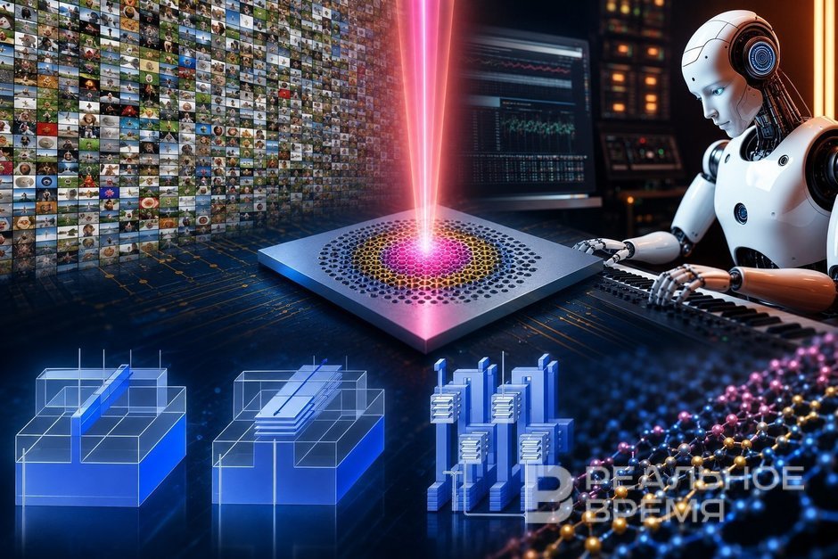
Microelectronics has crossed the nanometer threshold, photonics is solving the memory “bottleneck” problem, and neural networks have encountered an unexpected limit to learnability. In Realnoe Vremya's roundup— the main technological breakthroughs of the week that are changing the rules of the game in chips, energy, and artificial intelligence.
Is Moore's Law still alive?
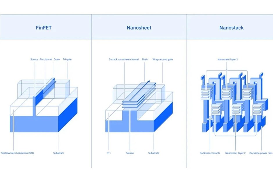
For the first time in the industry, IBM has pushed semiconductor development beyond the nanometer barrier. The company unveiled a technology that enables chip production with a 0.7 nm (7 angstroms) process node. The prototype, built on the Nanostack architecture, allows 100 billion transistors to be placed on a chip the size of a human fingernail — twice as many as IBM's 2nm chip presented in 2021. According to the company's estimates, the new process node will deliver either a 50% performance increase or a 70% improvement in energy efficiency compared to its predecessors.
But, as they say, the devil is in the details. The claimed 0.7 nm, like 2nm or 3nm process nodes, has long ceased to reflect the actual dimensions of transistors or even the distances between them. This is a marketing name for a technological generation, reflecting the level of performance rather than actual geometric dimensions. According to IBM's own data, the distance between transistors has remained at around 40 nm for many years and does not change in the Nanostack architecture. The breakthrough lies not in reducing physical dimensions, but in a fundamentally different approach to chip layout.
Instead of shrinking flat transistors, IBM engineers have developed a 3D architecture that stacks and shifts transistors relative to each other in a special way. Each transistor consists of three nanosheets 5 nm thick (about 15 rows of silicon atoms), separated by a 9 nm gap. This design allows different material combinations to be used on each layer, optimizing the performance and energy efficiency of each transistor independently of the others.
The progress in SRAM (static random-access memory) scaling deserves special attention here. It is used in central processors at the register and cache memory levels (L1, L2, L3). At the VLSI 2026 conference — the world's leading event for microelectronics professionals — IBM presented data on a 40% improvement in SRAM cell scaling. This could prove critical for AI accelerators, where it is often memory, not compute power, that is the bottleneck limiting throughput. IBM itself does not manufacture commercial chips but transfers the technology to partners — Samsung and Japan's Rapidus. The first commercial products on Nanostack technology are expected within the next five years. According to IBM estimates, this technology will remain relevant for at least a decade.
Optical computer memory
Modern photonic computers, which use light instead of electricity to process information, face a fundamental problem: they can transmit and process data quickly but cannot store it for long periods. The current storage system converts light “inside a memory cell” into an electrical signal and back again, negating all the advantages of optical transmission. Scientists from ITMO University (St. Petersburg) and Peking University have created a microscopic “trap” for light on a silicon chip to solve this problem, marking the first step toward full-fledged optical memory.
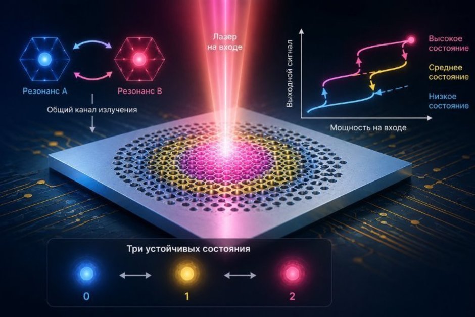
The development is a silicon structure less than 20 micrometers in size — thinner than a human hair. Its key feature is that conditions are created inside the chip where light waves begin to “get stuck” and repeatedly amplify each other. This allows light to be held in three stable states simultaneously. Unlike conventional electronic memory, which operates in only two modes (“0” or “1”), the developed cell can store more information in a single component. At the same time, the entire structure consumes only about a quarter of a milliwatt of power.
Moreover, the researchers fabricated real working samples and experimentally confirmed that the structure indeed functions as a multi-level memory cell. According to ITMO researcher Andrey Bogdanov, the technology can now already be used “as a platform for studying multi-level optical switching, optical memory, and other nonlinear photonic elements.” To create practical devices, however, “it will be necessary to solve the problems of scaling, integration with other photonic circuit elements, increasing speed, and reliability in more complex architectures.”
AI is losing its ability to learn
A study by Zypha has called into question one of the main dogmas of modern AI: that to create strong artificial intelligence (AGI), it is enough to simply scale up the model. Scientists have discovered that even large language models lose their ability to absorb new information over time — a phenomenon known as loss of plasticity. Increasing the number of parameters merely delays but does not prevent this effect, creating a fundamental obstacle for systems that must continuously learn throughout their “lifetime.”
By definition, AGI must be able to adapt to new data, tasks, and contexts without retraining from scratch. In the experiment, scientists trained eight GPT-like models — from 5 to 314 million parameters — on eight languages, switching them technically. Periodically, they checked how quickly the model mastered the previously unfamiliar Vietnamese language. It was found that all models eventually began to learn more slowly and worse. Moreover, loss of plasticity manifested itself even when the model was simply trained on a mixture of languages without abrupt transitions. The conclusion was that this phenomenon is not an artifact of task switching but a fundamental property of long-term training.

For an industry aiming for AGI, this means that the “just scale up” strategy has a ceiling. Even if we create a model with hundreds of billions of parameters, sooner or later it will stop effectively absorbing new facts, changes in language, code bases, or human preferences. In other words, creating AGI will require fundamentally new algorithmic solutions.
AI on the laws of physics
American startup Unconventional AI has introduced a generative model, Un-0, which operates not like a conventional neural network but as a physical system. Instead of billions of mathematical operations on a chip, it uses a network of connected “swinging pendulums” (oscillators) that, under the influence of each other, self-organize into the desired patterns and thus generate images. In essence, the developers have made the laws of physics work as a computational resource.
The main advantage of this approach is colossal energy savings. The company claims that Un-0 can reduce energy consumption for content generation by 1,000 times compared to current solutions based on graphics chips (GPUs). This becomes especially important against the backdrop of the growing energy crisis in the AI industry: data centers already consume as much electricity as small countries, and endlessly increasing their capacity is becoming increasingly difficult.

Currently, Un-0 exists only as a software simulation — the physical chip has not yet been created. However, the startup plans to release schematics for such a chip soon and build a full-fledged system based on it. In tests, the model showed quality comparable to early versions of Stable Diffusion. Despite a development team of fewer than 50 people, the startup has already attracted $475 million in investments from venture capital firms and Jeff Bezos at a valuation of $4.5 billion.